2024.02.15
News
“Printing” Photo-Thermoelectric Imagers on Soft Sheet High-yield All-Screen-Coatable Device Fabrication Process for Highly Durable Non-Destructive Inspection Use Camera Sheet
Non-destructive inspections play indispensable roles in rapidly growing industrial mass-production and social distribution in the borderless Internet of Things age.
Inspired by traditional art and clothing’s processing method “wood-block print,” the research group of Department of Electrical, Electronic, and Communication Engineering, Faculty of Science and Engineering, Chuo University, led by the Assistant Professor Kou Li, Professor Yukio Kawano, and the graduate student Yuto Matsuzaki fabricated the photo-thermoelectric imagers applying screen coating method. The fabrication method focuses on screen coating on large area of soft sensor sheet and the material inks, enhancing the durability. The study expects that combining various ink materials in the phase of screen coating extremely simplify integrated mount of multi-functional device substrate, which contributes to the manufacturing of highly durable image sensor sheets for non-destructive inspection use.
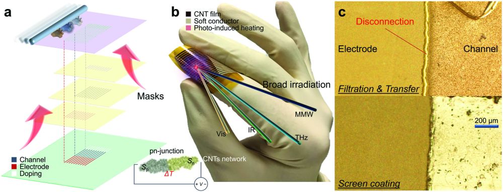
Figure 1. Conceptual diagram of the all-screen-coatable CNT film PTE imager. a: Schematic flow of the device fabrication. b: Multiple pixels-integrated ultrabroadband, soft, and thin 90 film image sensor array sheet. c: Durability comparison of the channel-electrode interfaces.
The research group has succeeded in developing a high-yield fabrication process of multi-functional soft photo-thermoelectric imager sheets by applying screen coating technology (Figure1/a.). The research group is developing the sensor as an element technology applied to multi-functional non-destructive inspection, which was originally focused and applied to the non-destructive inspection (term 1) technology such as “material identification (term 2),” “structural restoration (term 3)” that visualize interior materials assemblage or shape and layer reconstruction, without destroying three-dimensional structures (ex: in-vehicle components, medical tools, infrastructure equipment, animals, plants) consisting from various materials and structures. Conventional device fabrication process was the filtration & transfer method (term 4) which transfer and interface with each material such as sensor channel, doping solution, and electrode wiring only to the necessary part. However, the process was hindered by occasional disconnections between materials resulting in malfunction. The lack of the material’s mechanical robustness remained to be the issue.
In this study, the research team improved the fabrication efficiency and durability, thanks to the invented fabrication process of screen coating technology that forms all liquidized ink materials in a highly adhesive manner, which ended up controlling the device disconnections and malfunctions. This outcome will contribute to the large-scale aggregation and customized fabrication etc. required in the social implementation of photo-thermoelectric imager sensor sheet, and we expect further development of the application in the future.
The study report is released online on Advanced Materials Interface, as of Sept. 22, 2023.
*****************************************
【Researchers】
Kou LI, Assistant Professor, Chuo University, Faculty of Science and Engineering,
(Department of Electrical, Electronic, and Communication Engineering)
Yukio KAWANO, Professor, Chuo University, Faculty of Science and Engineering,
(Department of Electrical, Electronic, and Communication Engineering)
【The Research Information】
Journal: Advanced Materials Interfaces
Title: All-Screen-Coatable Photo-Thermoelectric Imagers for Physical and Thermal Durability Enhancement
Authors: Kou Li1,†,*, Yuto Matsuzaki1,†, Sota Takahara1, Daiki Sakai1, Yuto Aoshima1, Norika Takahashi1, Minami Yamamoto1, Yukio Kawano1,2,*
†Co-first author *Last Author
Affiliation 1Chuo University, Faculty of Science and Engineering, Department of Electrical, Electronic, and Communication Engineering 2National Institute of Informatics
DOI: 10.1002/admi.202300528
【Content】
1.Background
As the world is shifting toward the IoT society (term 5), the borderless society where human and things connect, the needs related to the technology of non-destructive inspection is surging. Among the existing several inspection methods, the photo-thermoelectric imaging technology is grabbing attention in terms of its characteristic of being able to acquire information from a large area and in a contactless way. Figuring it out by dividing into each frequency bands, optical radiation waves, the millimeter-wave (MMW), terahertz-wave (THz), and infrared (IR) regions (term 6) that locate between optical wavelengths and radio wave in particular, can identify non-metallic materials which most of industrial goods and infrastructures are made of, and expected to play a major role in non-destructive inspection techniques. The research group led by Assistant Professor Li has been working on to create a non-destructive inspection device system at the same bandwidth. Among them, the group has developed thin soft elastic ultra-broadband and high-sensitive MMW–IR, band image sensor sheet, ahead of the world, by using Carbon nanotube (CNT: term 7) membrane, Japanese-origin advanced materials, as device materials. (Figure 2. Reference thesis 1-3),
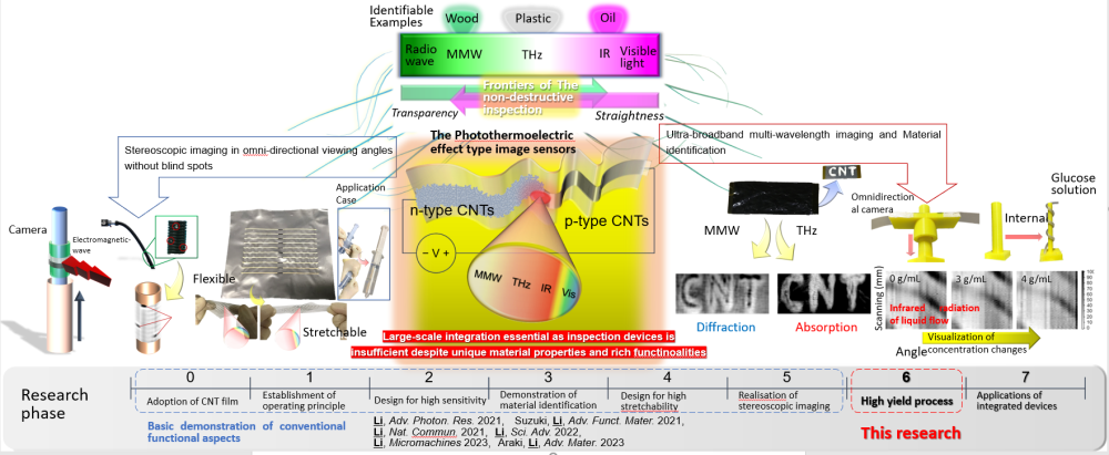
Figure 2 The research group worked on unique approaches up until this study (Reference thesis 1–3)
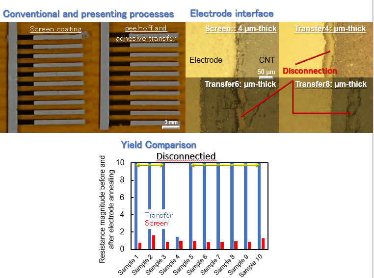
The research group is working on an inventive study in photo-thermoelectric development field owing to the devices’ optical properties and mechanical softness. Moreover, the study clarifies its competence as an inspection device through actually proving the non-destructive material identifications and structural restoration of target objects consisting of various materials and structures. (Reference thesis 4-5). On the other hand, the conventional device fabrication process was recognized as the cause of malfunction due to it being hindered by frequent disconnections between sensor CNT film and readout electrodes (Figure 3), and it had been a technical bottleneck for the large-scale aggregation such as camera implementation in the future.
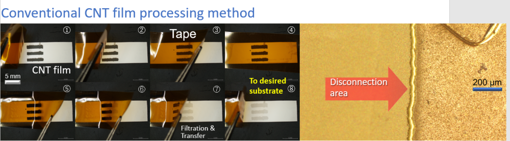
Figure 3 Conventional CNT film processing method (top) and optical microscope images of disconnection area (below)
2. Research and the Outcome
At first, the study investigated the cause of disconnections between CNT films and electrodes. As a result, it was found that disconnections attributed to conventional CNT film processing method (reference thesis 6) which filtrate material inks (CNT aqueous dispersions) to water-absorbing substrates using suction filtration film formation (term 8), and transfer to other functional substrates via adhesive tape depending on the device usage. In response to these findings, the research group led by Assistant Professor Li newly introduced the screen coating method as a method of CNT film formation which does not require filtration and transfer. The group got a clue from the coating method that “imprint ink into partial holes such as woodblock and printed T-shirt.” To begin with, the group prepared polymer mask of 25 µm thickness with a window cut out in the center through a laser process. This mask is placed on each substrates depending on needs, and the rotary bar imprints CNT aqueous dispersions on substrates through the window on the mask.
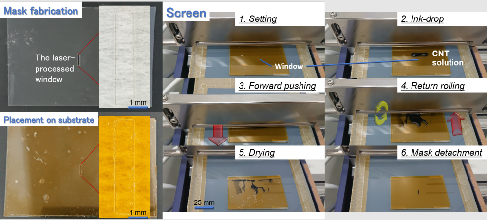
Figure 4. Element material ink coating method newly introduced in this research
In addition, the research group led by Assistant Professor Li also verified that the accuracy of screen coating is controlled by the viscosity of CNT aqueous dispersions (Figure 5). Under the conditions of low viscosity printing, the coating itself cannot be done or partial defects and non-uniform film thickness were found everywhere. On the other hand, in screen coating of ink concentration 0.5 wt%, which is the highest viscosity as of now, the group has succeeded in high-yield fabrication of CNT films approaching almost 100%. From the above mentioned, the study found that the ink viscosity can control the film quality and film thickness, as well as controlling the size and shape of CNT film formation at the coating window designing phase.
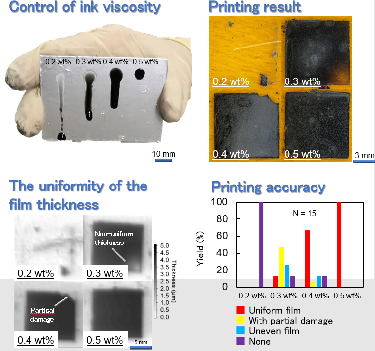
Figure 5. CNT film's viscosity control of screen coating method and its result
Furthermore, the research group led by Assistant Professor Li has not only established the CNT film fabrication process that does not require filtration and transfer which had been the issue to tackle in the preceding research, but also revealed that this screen coating contributes to the significant enhancement of its durability compared to the conventional trend of disconnections between electrode interface (Figure 6). The device is used to employ stretch type conductive paste to electrode wiring in order to leverage CNT film’s original softness, adding flexibility and stretching properties to not just the CNT film but the device as a whole. This paste is used as an electrode interface by thermal curing the unprocessed aqueous fluid, however, adjacent CNT film will be under load of tension due to the volume contraction arises when burnt. Then, Assistant Professor Li identified that the cause of disconnections of the conventional transferred CNT films was the loss of mechanical robustness when peeled off which resulted in failure to absorb a load, and verified that screen coating CNT film which strongly adhered to substrates show durability on volume contraction when burnt. Regarding the conventional process, the resistance prior and after burning which provides a stability index at CNT film/electrode interface surpassed 10 times among more than 90% of samples, and the disconnections trend was confirmed, however, the disconnections were prevented in every sample of the screen coating process. In addition, the resistance falls in the vicinity of 1 time which means the influence before and after burning has been controlled.
Furthermore, as a compilation of highly endurable and high-yield device fabrication process, the group succeeded in device aggregation of all-screen coatable photo-thermoelectric imagers and application to non-destructive device (Figure 7). Here, the study fabricated the 20-pixels integrated CNT film PTE image sensor array to confirm that all pixels move in high yield and the image visualizes the shape of the concealed knife, so that device original performance for non-destructive inspection is fully exerted.
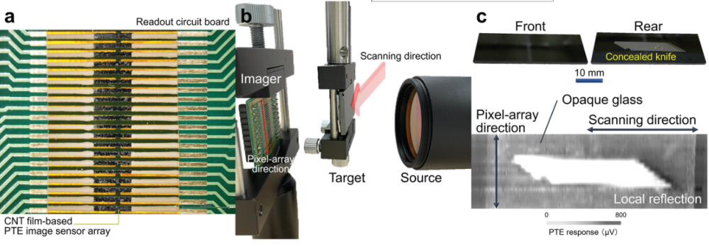
Figure 7. a: Mounting as an integrated devices, b: Experimental setup of transmissive one axial scan imaging, c: Application examples of the non-destructive transmissive scan
3.Future development
The research outcome is expected to be developed into screen coating of CNT film pixel camera sheet which is aggregated in large scale and high dimension for the two-dimensional flat. Currently, device evaluation is conducted mainly in single pixel or uniaxial pixel array, but the high yield multi-pixel aggregation will be possible on the foundation of screen coating high endurance process. We expect the non-destructive inspection screening will be developed into a video camera based real time movie which far exceeds the demonstration of current stop motioned imaging of non-destructive inspection. Besides CNT aqueous dispersions or conductive paste, the study also demonstrated the doping liquid inevitable in high sensitive photo-thermoelectric conversion, and the screen coating of isolation paste is inevitable in three-dimensional wiring intersection of electrode, so it is also adaptable to complicated aggregate structure when transitioning to camera. In addition, the mask used for coating is installable on various substrate surfaces such as plastic, glasses, and silicon wafers due to its adhesive feature and static electricity. This means CNT film imaging device aggregation can be implemented under the provision of various selections such as “plastic: thin and soft,” “glass: high transparency,” “silicon wafer: possible to combine with semi-conductor processing.”
To further accelerate this research, we need to work on to the further minimization of processed size. The size of the window on the mask printed will be reflected on each material’s sizes after, and the minimum as of now is 100 µm line width (about the same size as a hair). As the inspection device moves with great accuracy (ex: high-resolution imaging), tens of µm sized process and aggregation are required. By offering technical advantages in the laser process machine which is used in the fabrication of mask coating windows, we will put an effort to tackle these issues.
Screen coating is the method this study group has established which can be applied from anywhere under room temperature. In the future, we expect to develop an easy and available on-desk fabrication process for this non-destructive inspection camera sheet, in which CNT film’s material feature is applied at maximum, and requires no experience or techniques from the worker.
【Reference】
1. K. Li, T. Araki, R. Utaki, Y. Tokumoto, M. Sun, S. Yasui, N. Kurihira, Y. Kasai, D. Suzuki, R. Marteijn, J.M.J. Toonder, T. Sekitani, Y. Kawano, Stretchable broadband photo-sensor sheets for nonsampling, source-free, and label-free chemical monitoring by simple deformable wrapping, Science Advances 8, 19, eabm4349, 2022. DOI: 10.1126/sciadv.abm4349
2. T. Araki, K. Li, D. Suzuki, T. Abe, R. Kawabata, T. Uemura, S. Izumi, S. Tsuruta, N. Terasaki, Y. Kawano, T. Sekitani, Broadband Photodetectors and Imagers in Stretchable Electronics Packaging, Advanced Materials early view, 2304048, 2023. DOI: 10.1002/adma.202304048
3. K. Li, D. Suzuki, Y. Kawano, Series Photothermoelectric Coupling Between Two Composite Materials for a Freely Attachable Broadband Imaging Sheet, Advanced Photonics Research 2, 3, 2000095, 2021. DOI: 10.1002/adpr.202000095
4. K. Li, R. Yuasa, R. Utaki, M. Sun, Y. Tokumoto, D. Suzuki, Y. Kawano, Robot-assisted, source-camera-coupled multi-view broadband imagers for ubiquitous sensing platform, Nature Communications 12, 3009, 2021. DOI: 10.1038/s41467-021-23089-w
5. K. Li, Y. Kinoshita, D. Sakai, Y. Kawano, Recent Progress in Development of Carbon-Nanotube-Based Photo-Thermoelectric Sensors and Their Applications in Ubiquitous Non-Destructive Inspections, Micromachines 14, 1, 61, 2023. DOI: 10.3390/mi14010061
6. D. Suzuki, K. Li, K. Ishibashi, Y. Kawano, A Terahertz Video Camera Patch Sheet with an Adjustable Design based on Self-Aligned, 2D, Suspended Sensor Array Patterning, Advanced Functional Materials 31, 14, 2008931, 2021. DOI: 10.1002/adfm.202008931
The research was conducted with the supports from JST-Mirai Program (JPMJMI23G1), Japan Society for the Promotion of Science Grants-in-Aid for Scientific Research (Research A(JP23H00169), Research B (JP21H01746, JP22H01555, 22H01553), Grants-in-Aid for Transformative Research Areas A (JP21H05809, JP22H05470), Grants-in-Aid for Research Activity Start-up (JP 23K19125), Kanagawa Institute of Industrial Science and Technology/Strategic Research Seeds Fostering (Creation of non-destructive inspection use Smart Sheet), The Murata Science Foundation/Research-Aid (M23 194), as well as sample provision from Zeon Corporation.
(About the Research)
Kou LI
Assistant Professor, Chuo University, Faculty of Science and Engineering,
(Department of Electrical, Electronic, and Communication Engineering)
TEL: 81-3-3817-1860
E-mail: li★elect.chuo-u.ac.jp
Please replace ★ with @ when sending email.
Professor, Chuo University, Faculty of Science and Engineering,
(Department of Electrical, Electronic, and Communication Engineering)
TEL: 81-3-3817-1860
E-mail: kawano★elect.chuo-u.ac.jp
Please replace ★ with @ when sending email.
Chuo University, Research Support Office
TEL 91-3-3817-7423 or 1675 FAX 81-3-3817-1677
E-mail: kkouhou-grp★g.chuo-u.ac.jp
Please replace ★ with @ when sending email.
1. non-destructive inspection
Inspection technology that detects or visualize the occurrence of defection, transformation, and deterioration inside inspection object without "destroying substances."
2. material identification
Technology which individually identifies material combinations of composite inspection objects.
3. structural restoration
Technology which identifies an internal composition of inspection objects such as hollow, multi-layered, curved, etc.
4. The filtration & transfer method
The adhesive transfer from a membrane substrate to a tape. Besides adhesive transfer, the method using weak (van der Waals force,) which acts between molecules, is also reported.
5. IoT Society
An abbreviated word for Internet of Things. Under Iot Society, people and things are heavily connected. For example, applying total automation or wearable devices in the fabrication process and so on.
6. millimeter-wave (MMW), terahertz-wave (THz), infrared (IR) regions
Electromagnetic ray that located in frequency region from radio wave to optical wavelength. MMW is more low-frequency wave and infrared regions are more high-frequency light.
7. Carbon nanotube
Nanomaterial which was discovered by Dr. Sumio IIJIMA in 1991. It is composed of 100% atoms and nanometer size in diameter tube-shape.
8. Suction filtration film formation
A technique which extracts variance components and particles from the solution sample by dropping the liquid sample on the water-absorbing filtration substrate composed of cellulose acetate etc. and sucks air from the dropped surface and the opposite surface. There are micrometer sized tiny holes on the filter, after suction, a membrane of solution components is formed.
